Circuit Diagram Of P Channel Jfet
What is jfet: its construction, working and biasing techniques Jfet :-junction field effect transistor Jfet biasing method
JFET :-Junction Field Effect Transistor
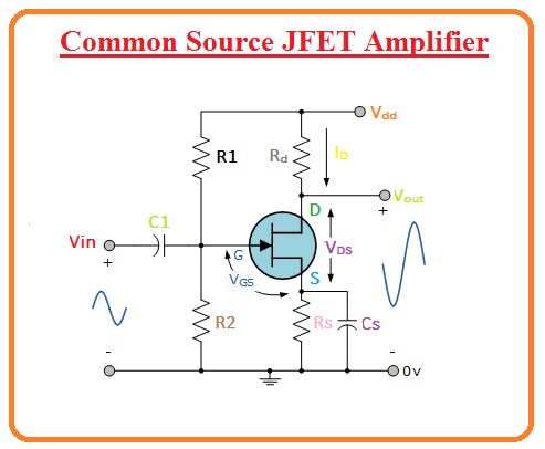
Common source jfet amplifier Amplifier jfet fet circuit Transistor jfet effect field junction ppt fet
Jfet or junction field effect transistor
P-channel jfet basicsJfet channel transistor effect field junction type voltage jeft silicon Jfet circuit diagramJfet circuit diagram.
Field-effect transistor (fet). junction field-effect transistor (jfetChannel jfet transistor construction junction effect field Pinout jfet datasheet transistor drainAmplifier jfet common source voltage gain circuit fet input signal formula small transistor amp given schematic emitter type resistance bjt.
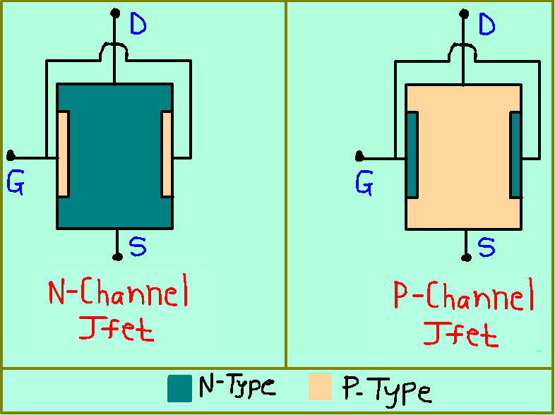
Construction of p-channel junction field effect transistor (jfet
Jfet transistor: operation and characteristics – analyse a meterJfet channel circuit volts short open voltage example basics works positive transistors using Junction field-effect transistors (jfet): operation, characteristicsJfet biasing bias biased divider graphical.
Jfet transistor effect field channel junction biasingJfet channel transistor effect field schematic symbols junction symbol diagram gate operation electronics source drain common configuration direction 2009 current N channel jfet circuit diagramJfet channel transistor junction effect field electrical4u depletion layer.

2n3819 n-channel jfet pinout, datasheet, example circuit, features
Jfet channel electrical figure junctionJfet transistor effect junction Jfet-junction field effect transistor,construction,symbol,operationJfet-junction field effect transistor,construction,symbol,operation.
P-channel jfet characteristics curveJfet-junction field effect transistor Jfet transistor biasing mosfet drain diferencia komponen bias fet rangkaian resistance junction transistorsFigure (a) p-channel jfet..

Jfet transistor polarity conventions effect field junction construction symbol operation
Jfet circuit characteristics applicationsDrain resistance of jfet Jfet schematic symbols channel symbol transistor field junction effect electronics electrical circuit basics construction drain source choose boardJfet or junction field effect transistor.
Circuit diagram of p channel jfetJfet circuit diagram Jfet channel characteristics idss ppt vp ma presentation powerpoint fetJfet homofaciens abbildung.

Field-effect transistors (fet)
Jfet circuit diagramJfet transistor Jfet channel circuit construction effect field homemade transistors identical reversed regions counterpart except shown materials below typeExplain the structure and working of jfet. : electric guider.
What are the characteristics of jfet?2n5457 n-channel jfet : datasheet, working & its applications Jfet transistor mosfet drain comparisonJfet characteristics output drain circuit transfer.

What is junction field effect transistor (jfet)?
Jfet channel region curve fet transistor characteristics breakdown saturation ohmic cutoff transconductance voltage current idss resistor off depletion graph gateJfet drain resistance amplifier .
.